Reducing Short-Circuit Power Dissipation in CMOS Inverters An LTspice Analysis
Ken Haine
Jul 21, 2024
In the first article of this series, we explored dynamic and static power dissipation in a CMOS inverter. In a subsequent article, we utilized LTspice simulations to further understand power consumption due to capacitive charging and discharging. As part of that discussion, we designed the LTspice inverter circuit shown in Figure 1.
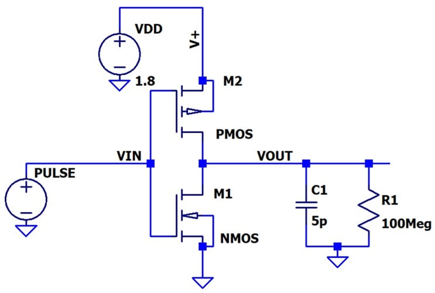
Figure 1. An LTspice schematic of a CMOS inverter with load resistance and capacitance.
We’ll continue using the above schematic in this article, which examines “short-circuit” or “shoot-through” current. These terms describe the current that flows through both the NMOS and PMOS transistors in Figure 1 during output transition periods.
Short-circuit current occurs because, as the input voltage—the gate voltage controlling the two transistors—changes, the inverter passes through a region where both the NMOS and PMOS channels are conductive.
Measuring Short-Circuit Current
To measure only the current flowing from 𝑉𝐷𝐷VDD to ground due to shoot-through, we must exclude the current that charges and discharges the load capacitor, C1, during transitions.
Short-Circuit Current During a Rising Output Transition
In Figure 2, we’ve zoomed in on the inverter circuit’s central part. The green dot at the drain of the NMOS transistor (M1) indicates the probe location for the low-to-high output transition.
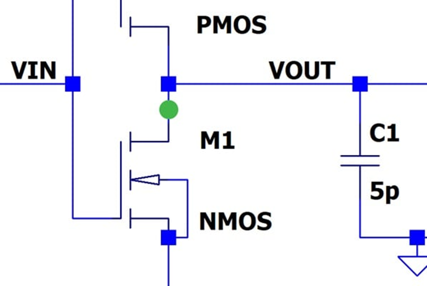
Figure 2. The green dot indicates where we measure shoot-through current as the output changes from logic-low to logic-high.
During a low–to-high output transition, charging current flows:
- From VDD.
- Through the PMOS transistor (M2).
- To the load capacitor (C1).
Meanwhile, short-circuit current flows:
- From VDD.
- Through the PMOS transistor.
- Through the NMOS transistor.
- To ground.
By probing the wire segment marked by the green dot in Figure 2, we measure the current flowing through the transistors after the charging current has diverted to the capacitor. The simulation results are shown in Figure 3.
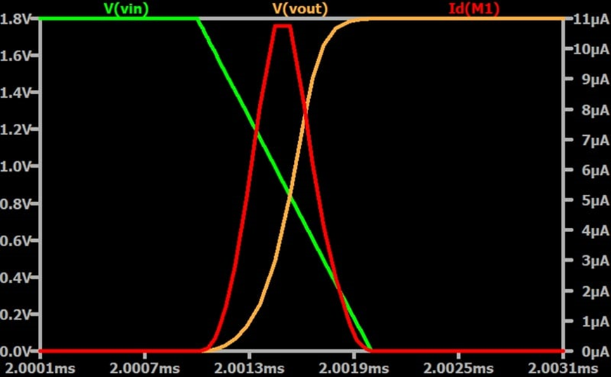
Figure 3. Inverter shoot-through current during a rising output transition.
The measured current peaks when the input is at 0.9 V. At this voltage, both the NMOS and PMOS transistors are weakly on. This allows current to flow directly from VDD to ground.
Short-Circuit Current During a Falling Output Transition
For the high-to-low output transition, the situation reverses. Discharging current flows:
- From the load capacitor.
- Through the NMOS transistor (M1)
- To ground.
However, the short-circuit current path remains unchanged, passing through M2 and then M1 to ground. Thus, we probe the current at the drain of the PMOS transistor, before the node where discharge current from the capacitor arrives. The probe location is marked in Figure 4.
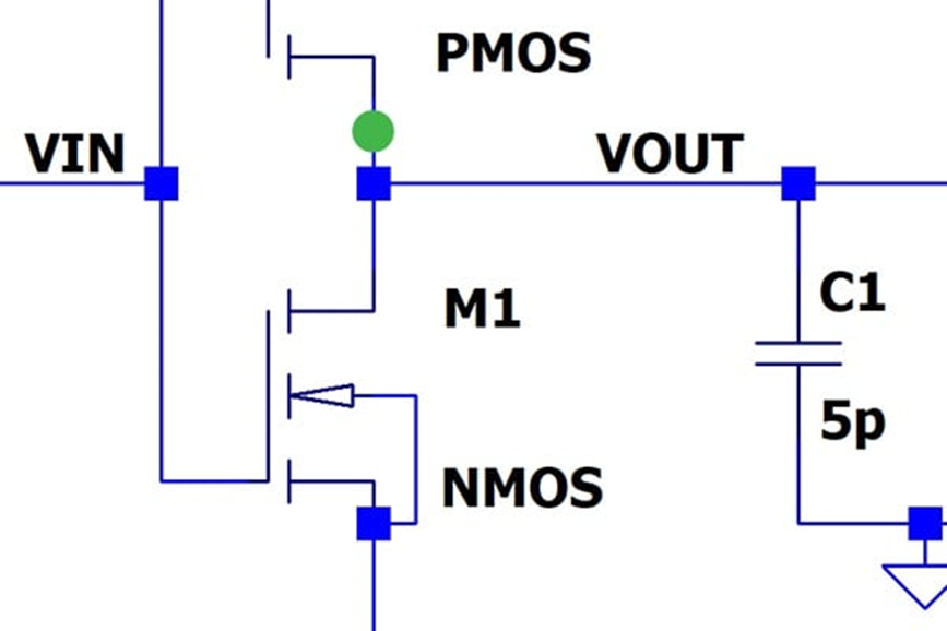
Figure 4. The green dot indicates where we measure shoot-through current as the output changes from logic-high to logic-low.
Figure 5 shows the LTspice simulation results for the falling output transition.
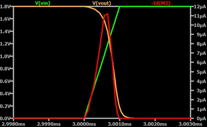
Figure 5. Inverter shoot-through current during a falling output transition.
Again, the current peaks when the input voltage is near its midpoint at 0.9 V. This short-circuit current causes power dissipation as it flows through the NMOS and PMOS resistance.
Measuring Instantaneous Power Dissipation
Two factors prevent us from easily converting our transistor current measurements into numerical power dissipation estimates:
- The current isn’t flowing through a fixed resistance, so we can’t directly apply P = I2R.
- The transistors’ drain-to-source voltages aren’t constant, so we can’t directly apply P = IV.
However, LTspice can perform the necessary calculations. Pressing the Alt key (Cmd on a Mac) while clicking on a component plots its instantaneous power dissipation. Let’s try this out.
The Rising Output Transition
The red trace in Figure 6 plots the power consumed by the NMOS during a low-to-high output transition. Since no charging or discharging current flows through the NMOS during a rising transition, this power dissipation results primarily from the short-circuit current.
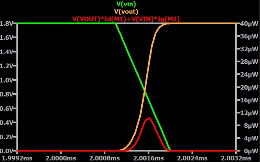
Figure 6. Instantaneous NMOS power dissipation during a low-to-high output transition.
In contrast, Figure 7 shows the instantaneous power dissipation for the PMOS over the same transition. Because charging current does flow through this transistor, its power consumption is significantly higher.
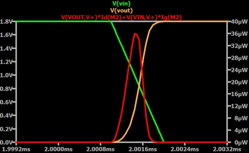
Figure 7. Instantaneous PMOS power dissipation during a low-to-high output transition.
The Falling Transition
For a high-to-low output transition, the capacitance current flows through the NMOS rather than the PMOS. The power dissipation of the NMOS (Figure 8) is now greater than that of the PMOS (Figure 9).
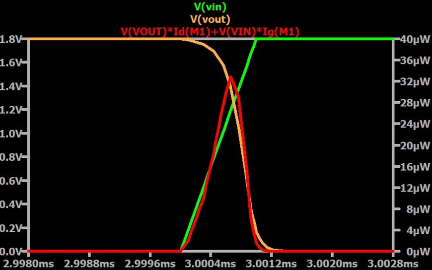
Figure 8. Instantaneous power dissipation of the NMOS during a high-to-low output transition.
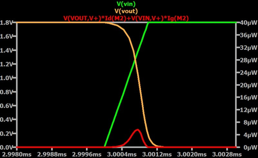
Figure 9. Instantaneous power dissipation for the PMOS during a high-to-low output transition.
For a falling transition, we examine the PMOS to find the inverter’s short-circuit power dissipation.
How Does LTspice Get These Results?
LTspice calculates power and displays the trace labels, showing the calculations. For example, the power dissipation for the NMOS (M1) during a rising transition is:
PM1=(VOUT×Id(M1))+(VIN×Ig(M1))
where Id is the transistor’s drain current (short-circuit current) and Ig is the gate current.
The power dissipation for the PMOS (M2) during the same transition is:
PM2=(V(VOUT,V+)×Id(M2))+(V(VIN,V+)×Ig(M2))
where V+ refers to the supply voltage (VDD in our original schematic).
In this case, the power dissipation is almost entirely due to the drain current. However, the presence of Ig in both equations reminds us that gate current can also contribute to total power consumption.
Energy Loss and Average Power Dissipation
Ultimately, the concepts and simulations in this article series aim to provide a toolkit for analyzing dynamic power dissipation in a CMOS inverter. In that spirit, I’d like to present one more piece of LTspice functionality before we conclude. While it won’t help us find out anything else about short-circuit power, it’s entirely relevant to the broader topic of dynamic power dissipation.
By holding Ctrl and clicking on the trace label for one of our instantaneous power waveforms, LTspice opens a cursor box. The bottom field in this box, labeled “Integral,” reports the energy lost over the simulated transition. For example, Figure 10 shows the total energy loss for the NMOS during a low-to-high output transition.
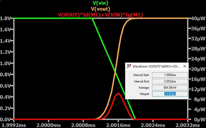
Figure 10. Energy lost through the NMOS transistor over the course of one rising transition.
Figure 11 shows the total NMOS energy loss for a falling transition.
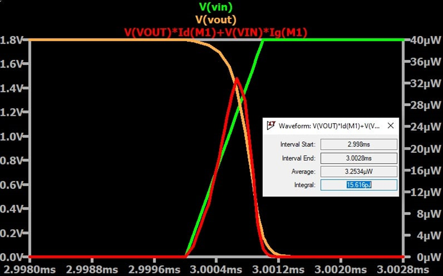
Figure 11. Energy lost through the NMOS during one falling transition.
Once we’ve found the total energy loss of the PMOS (Figures 12 and 13) as well, we can estimate the average dynamic power dissipation for our inverter.
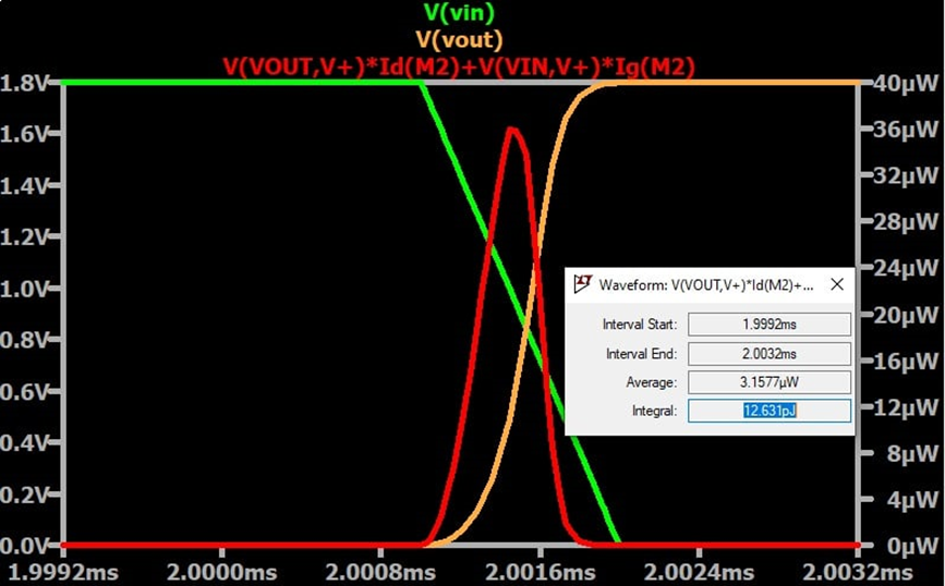
Figure 12. Energy lost through the PMOS during one rising transition.
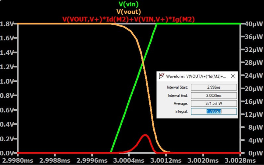
Figure 13. Energy lost through the PMOS during one falling transition.
For ease of reference, the energy loss values are reproduced in Table 1. Note the “Total” column on the right—we’ll use those numbers in a moment.
Table 1. Total energy loss of the transistors during one rising and one falling transition.
| NMOS | PMOS | Total (NMOS + PMOS) | |
| Rising | 3.563 pJ | 12.631 pJ | 16.194 pJ |
| Falling | 15.616 pJ | 1.784 pJ | 17.400 pJ |
We can now estimate the inverter’s average dynamic power dissipation as follows:
PAverage=(PRising+PFalling)×f
where f is the number of cycles per second.
For this simulation, we have PRising = 16.2 pJ and PFalling = 17.4 pJ. Let’s say the inverter is switching at 500 Hz. Recalling that one watt equals one joule per second (1 W = 1 J/s), this gives us an estimated power dissipation of:
PAverage=(16.2 pJ+17.4 pJ)×500 Hz=16.8 nW
With this information, you’re ready to experiment with techniques for reducing dynamic current flow and power dissipation in a CMOS inverter. This concludes my series on CMOS inverter power dissipation, though we may revisit these simulations in the future. In the meantime, I hope you’ve found our discussions helpful.
CATEGORIES
RECENT POSTS